Router? I Hardly Know 'Er - Part 2
This is a continuation of an older post series (well, can you really call a single post a series?) where I started using embedded/hardware pentesting techniques against some old routers I had lying around my place.
Unfortunately, due to some hectic moves in the interceding years, I’ve lost the original router I kicked off this series with.
Good new is I have no shortage of e-waste lying around my house at any given time, so we’re going to pick back up with a new router as a target: the Linksys WRT400N!
Profile of the Victim
WRT400N
This is another classic router from the mid-late 2000s, and there is still a ton of useful information about the internals of the router from hobbyist forums like the OpenWRT or DD-WRT boards.
Internal Photos
Chip ID
Right off the bat, we can see that there are three main ICs on the board. I looked up the other two smaller ones and found they were pretty uninteresting, so we’ll focus attention on the three highlighted components and two debug ports
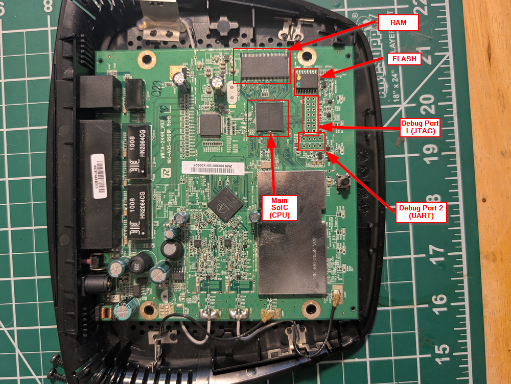
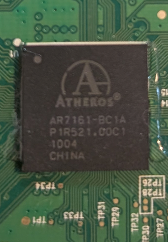
Main CPU
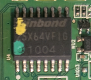
Flash Memory
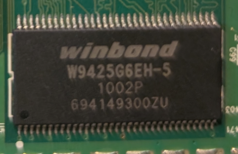
Dyanmic Memory (RAM)
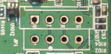
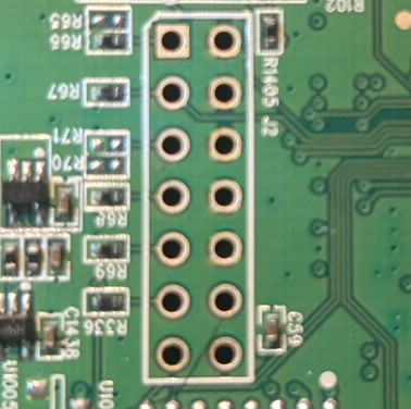
Debug Ports
Here’s port one (UART):
And port two (JTAG):
Open Source Intel (OSINT) Gathering
Just like last time, we’re going to do some OSINT to uncover any publicly available information about the device’s internals and the various chip datasheets. As a reminder, we are mostly interested in:
- Device’s make, model, serial number
- Schematic/spec sheets for identified Integrated Circuits (ICs) or other board components
- FCC ID and other regulatory OSINT
To summarize the info we’ve gathered from the device and our OSINT:
| Feature | Data |
|---|---|
| Serial Num. | MUJ00K307771 |
| FCC ID | Q87-WRT400N |
| CPU Type | Atheros AR7161 |
| CPU Speed | 680 MHz |
| Flash Type | Serial NOR Flash |
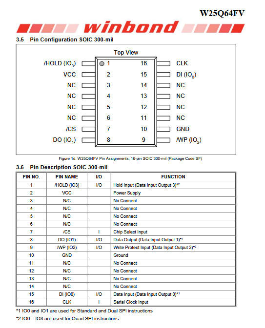
| Flash Chip | Winbond W25X64VF1G |
| Flash Size | 8 MB |
| RAM Size | 32 MB |
| RAM Chip | Winbond W9425G6EH-5 |
| Serial Port | Yes (UART) |
| JTAG Port | Yes |
Tigard
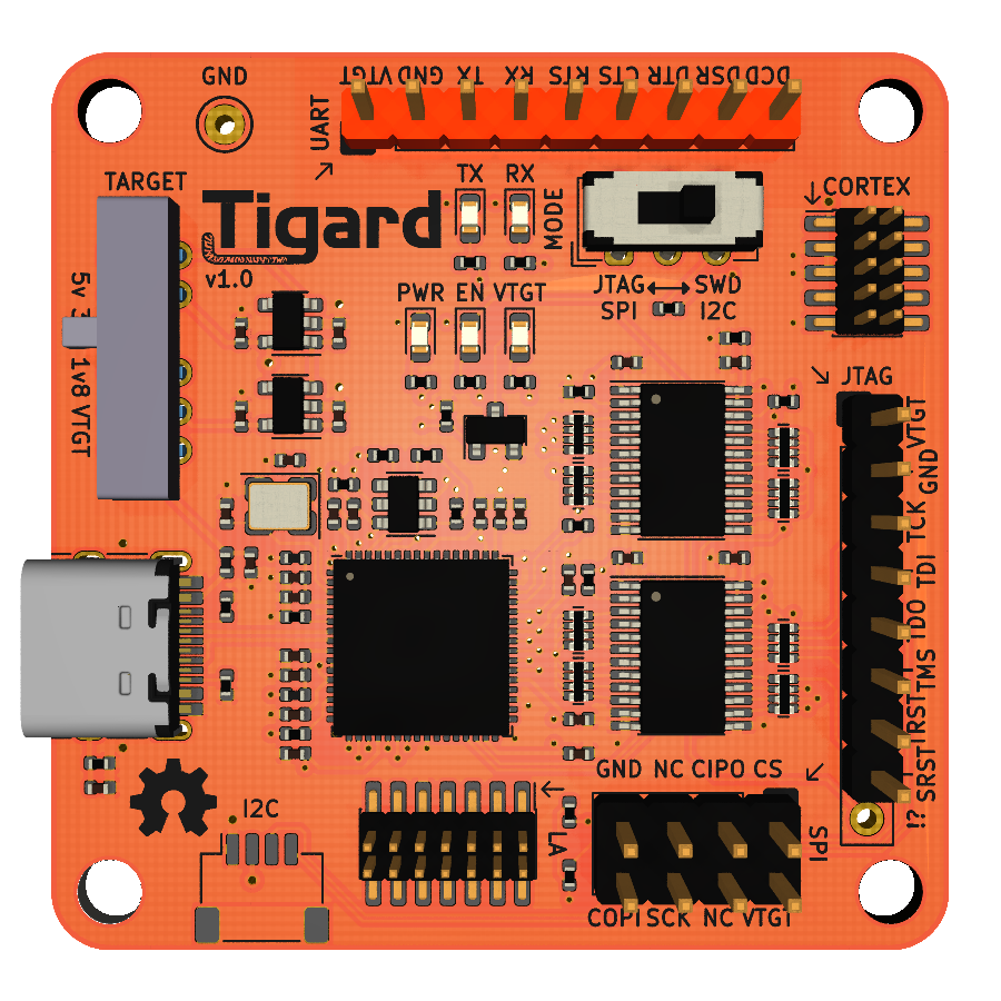
Instead of the buspirate, I figured I’d use my newest toy: The Tigard board! This board is based on an ft2232 chip, and features the ability to probe UART, JTAG, SPI, I2C, and more!
I acquired it as a part of the fantastic training available at securinghardware.com. Ironically, one of the best features is the color (bright orange), which makes it really easy to spot amongst all the other boards I have scattered about. Below shows the general layout of this debug board.
Exploitation
Since I’m not truly performing a penetration test of this hardware, rather just practicing some embedded/hardware hacking techniques, I’m omitting a formal writeup and breakdown of my methodology. This way, I can skip to the fun part directly (aka the Exploitation phase).
But without further ado, lets start mapping our attack surface!
UART
As we saw earlier, there’s a debug port with 4 pinouts suspiciously close to the main CPU…. who wants to bet thats a UART connection? The board also has the ground (G), transmission (T), and receiver (R) pins labeled! Making sure we connect Tx to Rx (and vice versa), our hookup looks as follows:
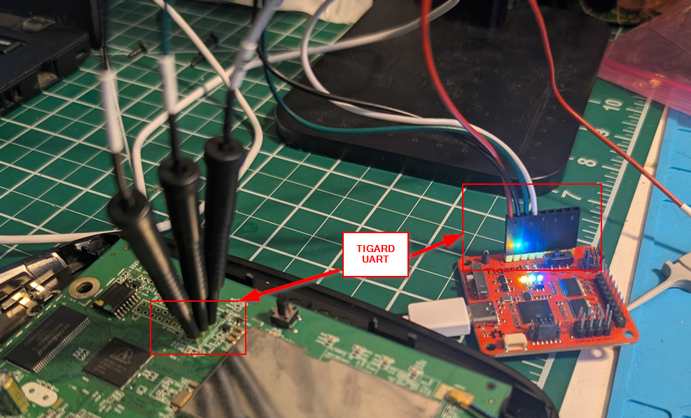
Now when we power on the device, we also start mashing the keys and spacebar to hopefully interrupt the autoboot process. We see that the boot interrupt worked, and we are dropped directly into a U-Boot shell directly interfacing with the AR7161 ARM CPU.
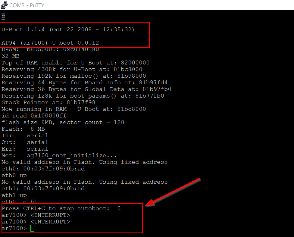
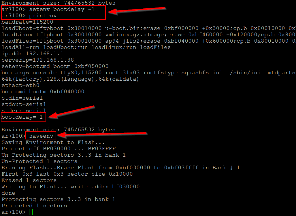
For a better quality of life while we poke around, we can adjust the boot delay value so that the device won’t autoboot into the main OS upon powering it on. looking up some U-Boot commands, we see that we want the printenv, setenv, and saveenv commands to adjust the bootdelay variable to -1.
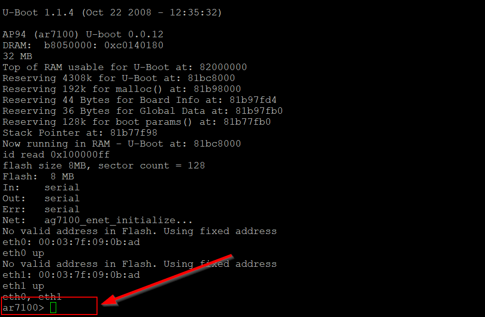
When we power cycle the device, we are now just dropped directly into the U-Boot shell and no longer have to mash to interrupt the process, as shown below.
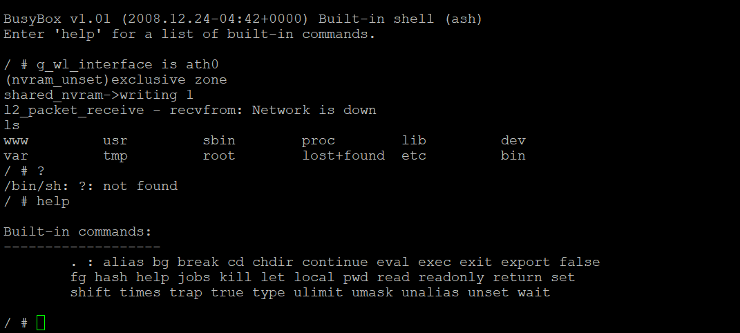
If we let the boot process fully complete, we see that the full device OS image is loaded from flash memory, and are presented with a Busybox instance complete with ash command shell access over UART. Effectively, we already have low-level root access over the device and the firmware it loads, but we’ll return to what we can do with this in a later post.
JTAG
Similarly, near the UART is another set of debugging pinouts. This is likely indicative of JTAG, but we’ll return to this port at a later date with JTAGScan and openOCD. For now, lets just proceed to our goal for today: dumping flash memory!
Dumping Flash over SPI
According to the datasheet, the flash chip for the device is a WinBond serial NOR flash, meaning we should be able to extract its contents through a standard Serial Periphery Interface (SPI) connection.
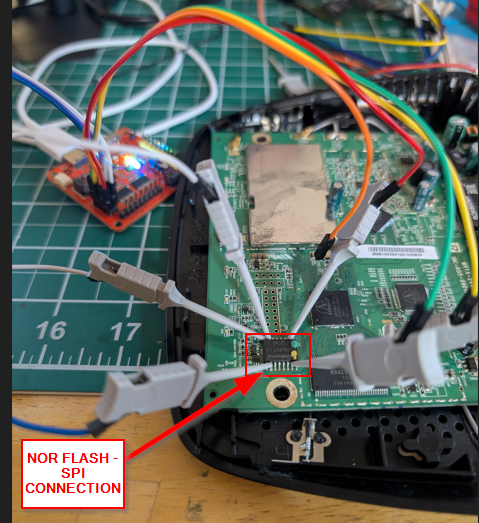
Using our Tigard board and some clipping hooks, we can directly attach to the pins on the flash chip and read the contents through SPI. Its always nice to have exposed leads to connect to. Often times modern boards use Ball Grid Array (BGA) pinouts to save space, but this makes attaching to chips on-board difficult. This is why I often enjoy using older boards/devices to practice, as the chip manufacturers are much more forgiving to the humble self-taught hardware hacker!
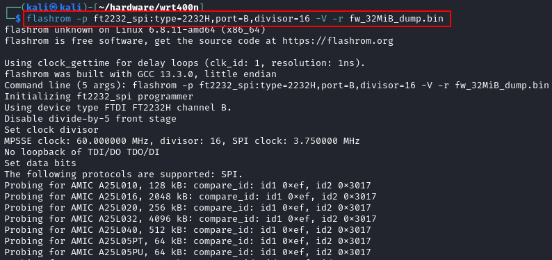
Once connected, I ran the flashrom command shown below to read the contents of the flash chip. As shown in the following screenshot, flashrom began by iterating through common chip manufacturer IDs to detect the currently connected chip.
flashrom -p ft2232_spi:type=2232H,port=B,divisor=16 -V -r fw_dump.bin
Eventually, flashrom identified the WinBond chip and dumped its contents to a file, as demonstrated below. Checking the datasheet is always a valuable step, as it can inform you as to the safe operating voltage and expected clock speed of the chip. If you are having issues with dumping chips through SPI, its likely that you are not respecting the values specified by the manufacturer.
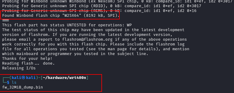
Now we have the contents of the data stored on the flash chip, but it is just a raw blob of data. We need to actually carve the contents out of this blob to proceed with our analysis. Fortunately, we should be able to use a tool like binwalk to extract the files out of this data blob, which we can then examine at our leisure.
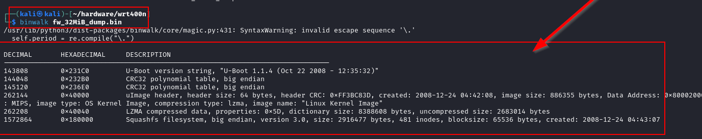
Recall that through our UART access, we learned that the U-Boot shell had a version number of 1.1.14 and indicated a compilation time of October 22, 2008. Based on that date/time, we can be pretty certain that we’ve extracted the contents of flash memory over SPI with no issues or file corruption.
From here, we would typically begin static analysis and basic disassembly of the recovered flash contents, and hunt for possible vulnerabilities on the device. I’ll return to that process as well at a later date. For now, a successful recovery is enough!
Final Thoughts
So in conclusion, the WRT400N is a really great device for practicing these various techniques. It had multiple debugging ports available, and a fairly accessible SPI-enabled flash chip which made dumping the contents a breeze. For next steps, we could leverage the access we’ve found to probe the firmware for vulnerabilities, or just fully replace it with a custom image with our root access to the bootloader.
Really, the world is our oyster! In the interest of brevity, I’ll stop here for now and maybe return with some fuzzing/vulnerability discovery within the firmware at a later date.
As a shout-out, I highly recommend the various hardware security courses available from the very talented Joe Fitzpatrick’s securinghardware.com site. I’ve been working through the part 2 of his hardware pentesting course and it is what inspired me to dust off these old routers and give them the business.